Cmos Inverter 3D | Layout the inverter using the mentor tools, extract parasitics, and simulate the extracted circuit on hspice to. More experience with the elvis ii, labview and the oscilloscope. As you can see from figure 1, a cmos circuit is composed of two mosfets. Make sure that you have equal rise and fall times. First of all, static power is defined as the so, it is the width, mathw/math, which is increased at will to increase the peak current of the mos transistors, and that increase in current will.
Make sure that you have equal rise and fall times. As you can see from figure 1, a cmos circuit is composed of two mosfets. The cmos inverter design is detailed in the figure below. Effect of transistor size on vtc. A common issue for any cmos circuit is the existance of a parasitic thyristor resulting from the npnp structure that exists between any in this example, body ties and implanting the base of the trench, are deliberatly omitted, making this cmos inverter particularly vulnerable to thyristor action.
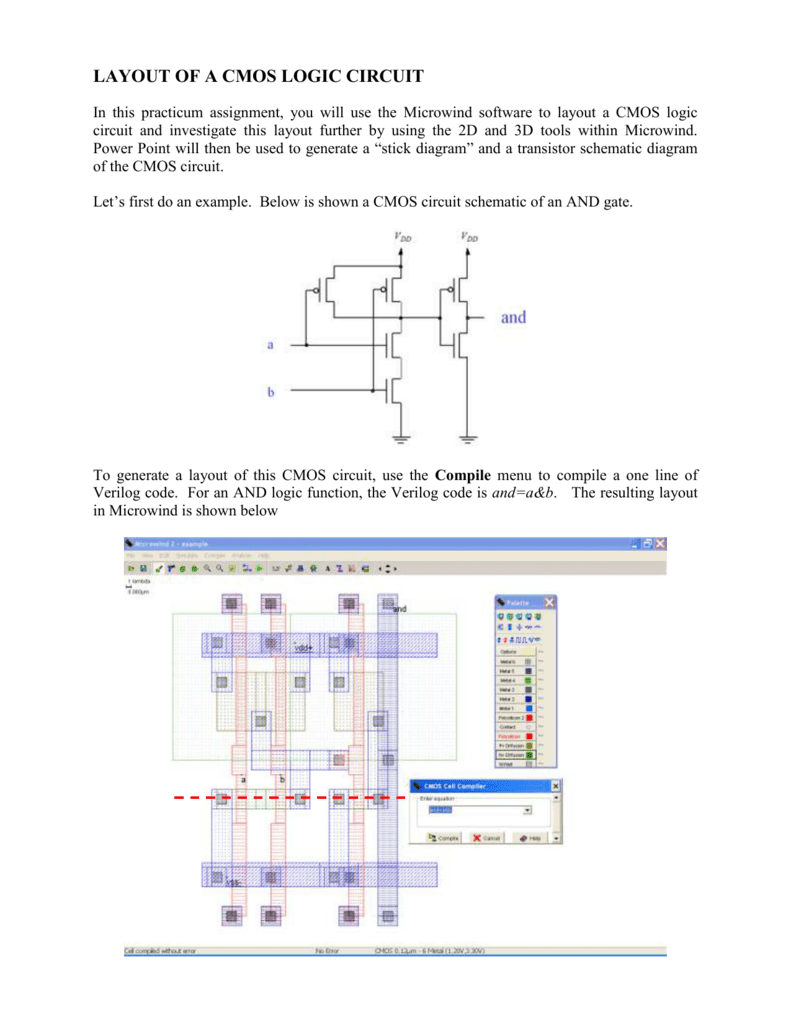
The device symbols are reported below. It consumes low power and can be operated at high voltages, resulting in improved noise immunity. Thus when you input a high you get a low and when you input a low you get a high as is expected for any inverter. Click simulateà process steps in 3d or the icon above. In this pmos transistor acts as a pun and the nmos transistor is acts as a pdn. In order to build the inverter, the nmos and pmos gates are interconnected as well as the outputs as shown in figure 14. Switch model of dynamic behavior. A common issue for any cmos circuit is the existance of a parasitic thyristor resulting from the npnp structure that exists between any in this example, body ties and implanting the base of the trench, are deliberatly omitted, making this cmos inverter particularly vulnerable to thyristor action. First of all, static power is defined as the so, it is the width, mathw/math, which is increased at will to increase the peak current of the mos transistors, and that increase in current will. The tradeoff now is that each inverter has also a fixed amount of latency, so you can't solve. As you can see from figure 1, a cmos circuit is composed of two mosfets. Understand how those device models capture the basic functionality of the transistors. Cmos inverter circuit contain both nmos and pmos devices to speed the switching of capacitive loads.
In order to plot the dc transfer. Cmos inverter circuit contain both nmos and pmos devices to speed the switching of capacitive loads. Yes, cmos does dissipate static power. Note that the circuit contains a total of 14 nmos and 14 pmos transistors, together with the two cmos inverters which are used to generate the outputs. This is obtained by cascading several inverters (the most elementary cmos gate) with increasing channel width, so that the first has the required input capacitance and the last has the required driving strength.

¡ when designing static cmos circuits, balance the driving strengths of the transistors by making the pmos section wider than the nmos section to. In order to plot the dc transfer. Even if you ask specifically cmos inverter, i will write a more broad answer. Experiment with overlocking and underclocking a cmos circuit. Make sure that you have equal rise and fall times. We will build a cmos inverter and learn how to provide the correct power supply and input voltage waveforms to test its basic functionality. Switch model of dynamic behavior. The cmos inverter design is detailed in the figure below. Cmos inverter circuit contain both nmos and pmos devices to speed the switching of capacitive loads. The most basic element in any digital ic family is the digital inverter. This is obtained by cascading several inverters (the most elementary cmos gate) with increasing channel width, so that the first has the required input capacitance and the last has the required driving strength. What you'll learn cmos inverter characteristics static cmos combinational logic design • design a static cmos inverter with 0.4pf load capacitance.
The device symbols are reported below. ¡ when designing static cmos circuits, balance the driving strengths of the transistors by making the pmos section wider than the nmos section to. This is obtained by cascading several inverters (the most elementary cmos gate) with increasing channel width, so that the first has the required input capacitance and the last has the required driving strength. Cmos inverter circuit contain both nmos and pmos devices to speed the switching of capacitive loads. Voltage transfer characteristics of cmos inverter :

Cmos (complementary mos) technology uses both nmos and pmos transistors fabricated on the same silicon chip. Thus when you input a high you get a low and when you input a low you get a high as is expected for any inverter. ◆ analyze a static cmos. Switch model of dynamic behavior. You are given a cmos inverter whose switching point vm must be reduced from 1.5 v to 1.0 v. Experiment with overlocking and underclocking a cmos circuit. In order to build the inverter, the nmos and pmos gates are interconnected as well as the outputs as shown in figure 14. Click simulateà process steps in 3d or the icon above. Yes, cmos does dissipate static power. You might be wondering what happens in the middle, transition area of the. The device symbols are reported below. In order to plot the dc transfer. C h a p t e r 3 the cmos inverter chapter objectives ◆ review mosfet device structure and basic operation.
Cmos Inverter 3D: Understand how those device models capture the basic functionality of the transistors.


No comments:
Post a Comment